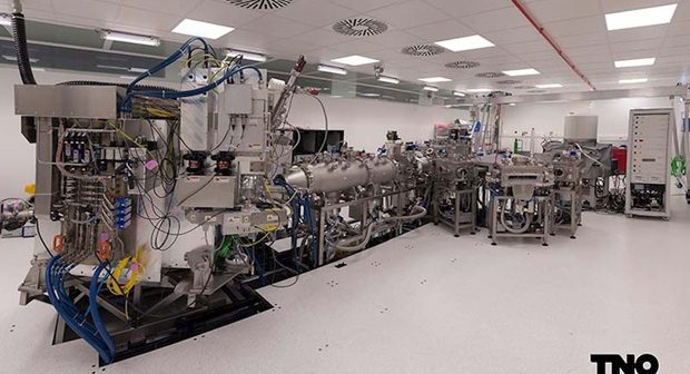
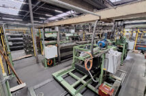
Andreas Dorsel, directielid van Carl Zeiss, en Paul de Krom, bestuursvoorzitter van TNO hebben gisteren EBL2 officieel in gebruik genomen. De EBL2 is een unieke en onafhankelijke analyse- en testfaciliteit van TNO in Delft die bij moet gaan dragen aan de realisatie van de volgende stap in chipproductie, met gebruik van EUV-licht. De eerste opdrachten zijn al binnen. Zie ook artikel in dat in de februari-uitgave van Link verscheen.
As EBL2’s name suggests, first there was the EBL(1), built in 2006. To keep improving the development of chips, the equipment to manufacture these chips has to become more advanced. With the introduction of Extreme Ultra Violet lithography, the need for a second generation of EUV test facilities increased. With EBL2, research assignments can be done 100 times faster, reducing turnaround times from months to hours. Another advantage of testing with EBL2 is that the experiments can be done outside the semiconductor factory, which shortens the development time of materials and components. In doing so, costs, risks and time to market are reduced considerably.
TNO designed and built EBL2 with national and international suppliers. Partners ASYS Automatic Systems and USHIO have made a major contribution with their knowledge and skills. Besides the construction, TNO has designed some unique parts of the EBL2 like the collector module, exposure chamber and sample holders. Dr. Dorsel, Board Member at Carl Zeiss, praised TNO at the opening ceremony as a reliable and very pragmatic R&D Partner with a proven long-term track record.
The funding for EBL2 has been provided by the Toekomstfonds (Ministry of Economic Affairs), NanoLabNL, EU framework Programme Horizon 2020 and TNO. The initial investment of about 10 million euros will be recovered over the next 10 years.
TNO’s EBL2 adds to the already flourishing ecosystem of world class opto-mechatronics in the Netherlands with not only ASML as prime example but with many related small and larger businesses and knowledge organisations.
