The Dutch photonics cluster is a variegated global centre of excellence. The ecosystem of researchers and entrepreneurs has acquired a leading position on basically all fronts. Innovative photonic ICs see the light of day there and can be produced ‘around the corner’ with stable front-end and back-end processes – on both the InP and SiN platforms. The Dutch cluster is also well advanced in making the Chiplet technology ready for the market, allowing both types of photonic chips to be produced quickly and cost-effectively.
Netherlands: variegated global photonics cluster
All in all, there are two major applications for integrated photonics: data communication (including telecom) and sensing. In the former, the US and China have a strong position. Companies like Intel, Lumentum and China Telecom invest large sums in technology to increase bandwidth and transport speed and to reduce energy consumption. As regards the latter, European companies and research institutes are leading the way in the development and production of photonic chips (pics) that use light (and the degree of reflection or scattering) to measure a wide range of things, from blood glucose levels to the presence of hairline cracks in metal. That is, for markets as diverse as medical diagnostics, automotive and aerospace.
Including telecom
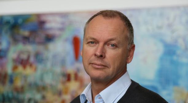
This is how Ewit Roos characterises the global photonics arena. He is the CEO of PhotonDelta, a public-private funded organisation that seeks to support the Dutch integrated photonics ecosystem in achieving a global position, for example by interconnecting Dutch photonics companies, research institutes and funders. He is therefore someone who can especially be expected to have a helicopter view of the world of photonics. He emphasises that the division into fields of application and centres of excellence is a very rough one. After all, his PhotonDelta recently participated in a €31 million funding of Eindhoven-based Effect Photonics. And this just happens to be a company which has developed – on indium phosphide (InP), a well developed ‘production platform’ in the Netherlands – a pic with which data can be transported over larger distances over different wavelengths. In other words: typically a solution that can be of great value precisely for the telecom world in which Europe occupies a relatively insignificant position.
‘The Dutch position here is so strong due in part to the development capacity, such as in the Photonics Integration Technology Center and in the very powerful supplying high-tech industry. A good example is Tegema in Eindhoven, which is developing back-end machines with which the Effect Photonics chip can be automatically connected in large volumes to the fibres for data transport. These innovations enable Effect Photonics to scale up quickly.’
Pics production
Smart Photonics, also from Eindhoven, supplies pics to the telecom market as well. This company, which was protected last year from a takeover by investors from ‘third countries’ by an investment of 35 million euros from the Dutch government, Innovation Industries, BOM and PhotonDelta and others, is a wafer production company that can produce any photonic chip, regardless of its application, for sensing and data communication. This company also works on the InP platform, which has the advantage that no separate laser light source is necessary. This makes these photonic sensors much more compact, cost-effective and energy-efficient. However, the fact that the government has set aside funds for this venture also has to do with the fact that Smart Photonics is a pure-play foundry: a factory without products of its own which – provided that the design meets all production requirements – can produce any photonic chip on that platform. ‘In that respect you can compare Smart Photonics with chip manufacturer TSMC, only many, many times smaller. Other fabs like NXP do carry their own products and so are not so readily hired by competing chip designers.’
Equipment construction
The front-end machine construction for this branch is developing less rapidly because of the fact that InP chips can be produced very well and in large numbers on existing semiconductor machines such as ASML’s mature wafer steppers. ‘The differentiating factor lies above all in the knowledge of how to use this production technology: how to adjust the wafer stepper to produce high-quality wafers as quickly as possible. Smart Photonics has precisely that knowledge.’ The competition between machine builders mainly takes place on this back-end market, with machines that connect these photonic ICs to the outside world as well and as quickly as possible (packaging). ‘Seventy percent of the cost of a pic component is still in backend production. This obviously has a major impact on the cost and hence on a component’s market penetration’, says Roos. Tegema is active in this field, and so is Enschede-based Phix Photonics Assembly. Phix’s technology distinguishes itself by being platform-independent: pics produced on the InP platform, on the silicon nitride (SiN) platform as well as on the silicon (Si) platform can be packaged using this company’s technology.
Strong InP and SiN value chain
From his account it becomes clear that the Dutch photonics cluster is very strong in the entire InP and SiN value chain, from designing these chips to producing and packaging them. However, which platform will be the leading global platform for photonic chips is by no means yet a foregone conclusion. These are definitely platforms on which pics for a wide variety of applications, for data communication and sensing, can best be produced. But still in limited volumes, according to Roos. ‘The third type, Si-pics, is the easiest to produce in large volumes. After all, this is the same platform on which the TSMCs and the Samsungs have been making ordinary, electronic CMOS chips on a very large scale for decades.’
Leading platform?
The so-called Chiplet technology now under development combines the best of multiple platforms. ‘This hybrid technology makes it possible to combine functional blocks made on one platform with blocks made on another. Phix, together with Tegema and the Chip Integration Technology Center, is well on its way to developing this technology. Using money from the National Growth Fund (a €20 billion, five-year government-funded fund for investments that contribute to economic growth, ed.), we hope to be able to further expand the existing leading positions throughout the InP and SiN value chain, by such means as intensification in Chiplet technology’, says Roos in conclusion.
The equipment builder: Dutch demand will grow

Pierre van Lamsweerde expects the Dutch demand for production solutions to grow considerably in the coming period. Photo: Tegema
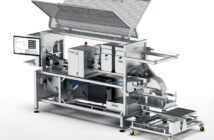
The southern Netherlands region is strong in innovating photonics technology. However, the customer base in this segment for production solutions is smaller than he had anticipated, admits Pierre van Lamsweerde of Tegema Etteplan. This Eindhoven-based multidisciplinary system integrator has developed and built a modular micro-assembly platform. The photonics sector in the south of the Netherlands could use it, for example, to connect integrated optical chips to fibre optics, which are used in, for example, telecom and automotive.
Not that there is no market in the Netherlands, Van Lamsweerde hastens to add. For a telecom application, Tegema Etteplan is working together with Effect Photonics that has developed a technology to increase the capacity of existing fibre optic networks. Phix in Enschede, a company that specialises in the packaging of optical chips, is also an important partner of Tegema. Together with the Chip Integration Technology Center (CITC) Tegema founded the photonics consortium Podium, to improve the assembly of integrated phonics. CITC is a research institute specialising in semiconductor packaging technology with TNO, the largest Dutch research institute, as its founding partner. ‘The market here is not big yet. But it is sizeable enough to be able to learn from the customer’s experiences. This will allow us to further accelerate and standardise our production technology.’
Van Lamsweerde expects the Dutch demand to grow considerably in the coming period because the scalable photonics market is ‘very much on the up’. This applies to the customers mentioned, but also to Photon First (until recently operating under the name Technobis), which just set up shop at the High Tech Campus Eindhoven.
In the meantime, Tegema is spreading its wings towards China and the US. And it helps that since last autumn, the Eindhoven-based company has been part of Finnish multinational engineering firm Etteplan. ‘This makes it easier for us to internationalise. For example, we are now talking with Intel in the US. If you tell people that you are part of a company of 3,000 engineers, continuity is no longer an issue for them, and from then on you’re only talking about your technological competences.’
The investor: money in products and infrastructure

Nard Sintenie
Innovation Industries invests in high-tech mechanical engineering, robotics, foodtech and integrated photonics. Four areas in which Dutch industry excels, says general partner Nard Sintenie of the venture capital fund. ‘As for photonics: if you look at the number of researchers at our universities of technology and knowledge institutes TNO and Imec, which are working on this, and at the number of patents and citations in this field, you can’t but conclude that the Benelux is a photonics centre of excellence worldwide.’
All these efforts naturally lead to applications that can generate economic and social value. However, most investors are not queuing up for it, observes Sintenie. ‘Many investors only know about money and the market. They don’t understand the technology of a spinoff company and so they don’t join. If you want to invest successfully in technology, you have to be able to understand it. We can do that because there are sixteen of us and almost all of them are techies.’

Theo Kneepkens
(KLA) about supercycle of growth: Í hope that supply industry expands its capacity’. Read this edition of link magazine digitally via this link
With that baggage, Innovation Industries has built a portfolio of eighteen high-tech companies, three of which operate in photonics. Two of them, Smart Photonics and Phix, provide the infrastructure for the companies dedicated to photonics products. ‘For photonics product companies to be successful, they had better not be dependent on a foundry somewhere in Taiwan. You need to be able to coordinate quickly and effectively with a company around the corner in that case. That’s why we invested in that infrastructure and simultaneously started investing in a product company.’ By which he means Effect Photonics, the third photonics company in Sintenie’s portfolio. Are more of such investments likely to follow soon? ‘Me and my partners are constantly looking for it.’
And none of this is done with the intention of divesting these companies as quickly as possible for profit. Innovation Industries, which also makes use of European and Dutch government funding, keeps a close eye on the European and Dutch economic and social interests, Sintenie explains. ‘We build companies until they have a strong position in the global market and in the Dutch ecosystem. The sale of such a mature business does not lead to relocation out of the Netherlands, but usually to more investments by the new owner here. Accordingly, we assume an investment horizon of 12 years, much longer than that of the average venture capitalist.’
